Vanishing Point v2.1
Updated Vanishing Point
Introduction
With the release of the Vanishing Point v2.0 many new features and improvements were made but there still were various problems with the circuit. I decided take some time to resolve all the outstanding issues with v2.0 and add a few more features. This resulted in the Vanishing Point v2.1 (Figure 1). This article will cover the updates made to the circuit. The same basic operational principals of v2.0 still apply so read that article as well as this one to understand fully how the circuit works.
Note: Vanishing Point v2.0 can be upgraded to v2.1 with a little work. Most of the changes involve the off board wiring.
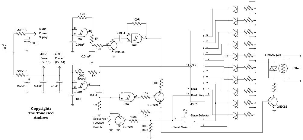
Figure 1
Random Mode
Vanishing Point v2.0’s random mode had some issues. Enough so that some people would even avoid building the circuit with the random mode due to the difficulties. Those issues have been addressed with v2.1.
Optocoupler Replacement
The random mode used in v2.0 works well when tuned right but one of the biggest problems with v2.0 was the optocoupler. The lack of accessibility to a common optocoupler made it difficult to construct the circuit. The behaviour of the circuit would vary a great deal depending on the optocoupler so it was next to impossible to give a specific set of values that would work well with the circuit. I decided to eliminate the optocoupler and find another method.
The principal that v2.0’s random mode uses works well so the same concept was kept while adapting the circuit to use more common parts. The main function of the optocoupler in v2.0 was to vary the speed of the High Frequency (HF) clock with the changing voltage from the modulation (mod) clock. The clocks used in the circuit are simple R/C based clocks which there are a few ways to change the clock speed.
One of the most common ways to change the clock speed is to vary the amount of output feedback to the input. This is usually done with a variable resistor like a pot. This is what the pot in the sequencer clock does for example. It is also what the optocoupler does in the HF clock only the pot is replaced with the optocoupler’s LDR. Another way to vary the speed is control the capacitor’s path to ground. This method would remove the need of a specific range of values for the optocoupler’s LDR and feedback resistance.
To vary the capacitor’s path to ground through the means of a control voltage a transistor is placed in series with the capacitor to ground (Figure 2). As voltage is applied to the input of the transistor, as from the mod clock, it will increase conduction to ground thus changing the speed of the clock.
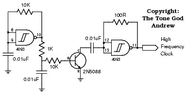
Figure 2
The transistor model should not matter too much. I used a 2N5088 originally but I also substitute 2N5089s, 2N3904s, and other transistors with no problems. Just about any similar transistor model should do. This should resolve the part sourcing issues that the optocoupler caused.
An added advantage of replacing the optocoupler with something more predictable is now various part values can be specified for more consistent results. The resistor in the HF clock can now be set to a value that produces a high enough speed. The mod clock values can be specified as well. The values I have suggested seem to work well over a wide range of voltages and sequencer clock speeds. Of course you can still adjust various values to your taste using the Vanishing Point v2.0 article as a guide but now you can do this with the added comfort that your selected values will work consistently if you build more then one Vanishing Point v2.1.
Beat Feature / Random Rotation Suppression
Another big problem with v2.0 was tuning the random clocking period that came from the HF clock which quickly clocked the stages for a very short period of time to produce the random result. Too short a clocking period would not produce a good result. Too long a period and the HF clocking would become visible/audible on the stages.
To resolve the problem it would be simplest to turn the stage/optocoupler LEDs off during the random clocking period. Placing a NPN transistor in series with stage/optocoupler LED’s ground path allows the turning on and off of the LEDs (Figure 3). This transistor is controlled by the pulse detector output which is low during the random clocking period thus turning off the LEDs and on the rest of the time.
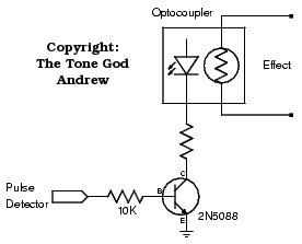
Figure 3
Another behaviour that occurred during random mode was when the same stage got selected after the random clocking cycle it would hold the stage almost solid with no break in between clocking cycles. I felt this broke the rhythm of the sequencing so it was not very musical sounding. With the stage/optocoupler LEDs now controlled from the pulse detector the random clocking period could be extended so in between clock cycles the LEDs would be turned off longer thus creating a “beat” even when the same stage was selected after the random clocking period.
An added bonus of this is that the longer random clocking period gave the HF clock a chance at more clock cycles/stage steps thus producing a better random result. Adjusting the random clocking period is easier as well as there is no more concern of the LEDs glowing from the HF clocking since the LEDs are turned off during the random clocking period. This is a nice way to eliminate two problems with one solution.
Simplified Switching
Switching between sequence and random modes until this point required large switches and complex wiring. I found there was a easier way to switch between modes.
One slightly under documented behaviour of the 4017 is when the clock input (pin 14) is set high and the enable/inhibit input (pin 13) is clocked the output will step. This allows the enable/inhibit input to be used as a second clock input if the clock input is high.
The sequence clock can then be connected permanently to the clock input reducing the need for a pole in the sequence/random switch. The HF clock could be hooked up to the enable/inhibit input to clock the 4017 during random clocking periods. Doing this brings back the problem of the random clocking cycle occurring for 50% of the time since the sequence clock has roughly a 50% cycle and a high on the clock input would allow the HF clock to step the 4017. Placing a transistor on the enable/inhibit input connected to ground with a resistor to the HF clock output (Figure 4) allows the disabling of the HF clock by grounding the enable/inhibit input when the transistor input is high.
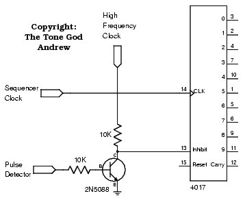
Figure 4
To enable the HF clock on the enable/inhibit input for the random clocking period the transistor’s input should be low. The pulse detector gives the random clocking period so we can use the pulse detector’s output much like what was done in v2.0 with the 4017’s enable/inhibit input. When the sequencer clock feeding the 4017’s clock input and the pulse detector goes high it will activate the enable/inhibit input’s clock behaviour at the same time enabling the HF clock for the random clocking period. The pulse detector will also switch off the LEDs during the random cycle period producing the beat/rotation suppression feature. Using the pulse detector output to control both the HF clock enable and the output LED’s makes sure everything is synchronized.
Lets look at how to switch to the sequence mode from random mode. You could disable the random feature by setting the transistor that controls the HF clock to high which would disable the HF clock. This will work but the beat feature would still occur on the output LEDs. I find that the beat feature when enabled during the sequence mode diminishes the “smooth” stage stepping. Having the output LEDs on all the time through the stepping sounded much better musically. In order for the output LEDs to be on all the time for the sequence mode the LED switching transistor’s input must be high. At the same time for sequence mode the HF clock must be disabled which is done by setting the HF clock enable transistor’s input high.
So after all that where is this “simplified switching” I spoke of ? The LED switch transistor and the HF clock enable transistor are both connected to the pulse detector so setting the detect output to high will enable the sequence mode. Setting the pulse detector’s output high can be achieve by grounding the pulse detector’s input (Figure 5). This results in a high output driving the transistors into the appropriate state. The sequencer clock is protected from shorting by the pulse detector’s input capacitor. The sequence/random mode switch can now be a SPST toggle switch connected to ground. Yet another simple single solution that resolves two problems.
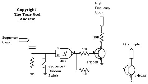
Figure 5
Reset
There were some minor problems with the reset circuit so here are the corrections to solve those problems.
Spontaneous Resetting
Under certain conditions the sequencer would go back to stage one randomly. The reason for this is that when all ten stages are active the reset pin (pin 15) is left floating. The reset pin when left open can pick up noise from the surrounding environment. Noise which would sometimes be enough to trigger the reset. This is resolved with a pull down resistor on the reset pin (Figure 6). A value of 10K-100K should be sufficiently low enough to filter out noise when the reset pin is left open while not interfering with the normal operation of the reset pin being triggered by the stage output(s).
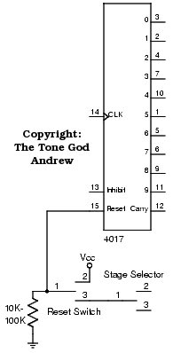
Figure 6
Blinking Stage LED During Reset
One side effect of the enable/inhibit input clock trick is that when in the random mode and activating the reset input the stage LED would blink at the rate of the sequencer clock. If you are using the bypass switch to hold at stage one while bypassed then the LED will just blink. While this does not affect the output it does look funny. If you are using a separate switch to manually reset and hold the position while the effect is engaged this could cause audible problems.
This behaviour does not occur when in sequence mode so a quick solution is to force the circuit to go into sequence mode when being held at reset. This can be done using transistor connected to ground attached to the input of the pulse detector’s input (Figure 7) much like the sequence/random mode switch. The transistor’s input is connected to the reset pin so when the reset goes high the transistor will ground the pulse detector’s input putting the effect into sequence mode.
Figure 7
This will not affect the stage selector feature as the reset pulse is so quick that you won’t notice the mode changes.
Modifications
There are some commonly requested modifications. I’ll cover them quick here.
Speed Indicator LED
It maybe helpful to have an LED that blinks in time with the sequencer’s clock. It is particularly useful if the stage outputs are set so low you can’t see the stages moving. If you have used the “bypass/sit at stage one” mod you can see the speed while the effect is bypassed.
You could try connecting a LED directly off the sequencer clock output but you have to be careful of the amount of current the LED would pull as it could load down the sequencer clock output to the point that it will not be able to clock the 4017.
If you have a spare gate sitting around, for example you used a 40106, or if you can fit another transistor in the circuit you can use the sequencer clock output for a gate/transistor which would drive an LED (Figure 8 and Figure 9). That is a much better way to do it.
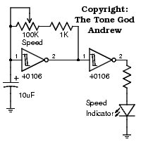
Figure 8
Figure 9
Manual Step Mode
I mentioned in earlier Vanishing Point versions that you could modify the circuit to be able to step through the stages manually. This is easy enough to do.
With the simple sequence/random mode switch a DPDT switch can be used for the manual/clocked mode switch with one pole connected in series with the sequence/random mode switch. This can force the circuit into sequence mode regardless of the sequence/random mode switch state. The other pole of the manual/clocked mode switch will disconnect the sequencer clock from the 4017’s clock input and connect the manual step switch.
The 4017’s inputs have schmitt triggers on them. This makes debouncing the step switch input real easy. As covered in the Follow The Debouncing Ball article you can use a simple R/C network feeding a schmitt trigger input to debounce the switch. A connection to ground on the 4017’s clock input will step the output one stage.
If you want a stand alone step switch you can use a momentary SPST switch. If you want to use the sequence/random mode switch to step the sequencer then you will need a DPDT toggle switch. Connect the center pole to the 4017’s clock input and the outer poles to ground (Figure 10). When the switch is depressed the gap that occurs during the physical switching between contacts generates a clock pulse for the 4017’s clock input stepping the output.
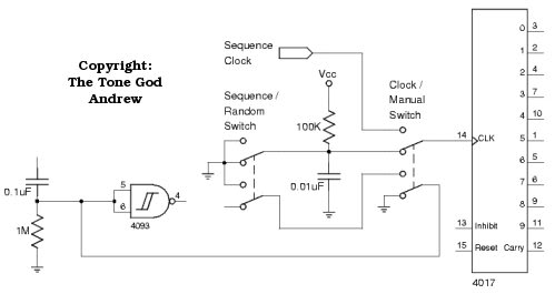
Figure 10
Noise Reduction Techniques
Interfacing digital circuitry to analog circuitry can very easily create noise problems. This time around I included some of the noise reduction circuit as part of the schematic so people don’t forget and more importantly understand how to it.
Power Supply Isolating
The high speed switching the logic gate do the sudden power spikes could work their way into the audio via the power supply. It is a good idea to isolate the digital power supply and analog power supply. This is accomplished by placing a resistor, between 100ohms and 1K, in series with the power supply coming in and the digital power supply. Right after that resistor a large capacitor, roughly 100uF, is placed connecting to ground. This then feds the digital supply. The same thing should be done for the audio supply if needed. (Figure 11)
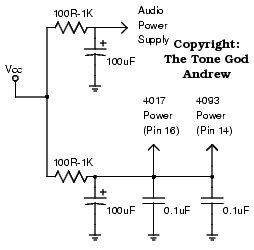
Figure 11
Decouple Logic ICs
With all this high speed switching going on other anomalies can occur including spikes that can cause a change in logic state(s). It is a good idea to decouple the power supply to each logic IC. A simple ceramic capacitor, 0.1uF or so, connected from the power supply to ground located as physically close as possible to the IC should work.
Ground Connections
It is a good idea to keep the grounds used for analog and digital separate from each other. The analog circuit should have it’s own set of ground connections and so should the digital circuit. Within each circuit all the ground should connect to one location as a central ground point.
After each circuit section has it’s ground connections take the central ground point of each circuit and connected the two sections at one point only. A jack connection is a good place to do this.
Ground Plane
If the audio and digital circuits are close to each other you may wish to place a ground plane between the two sections to prevent noise form radiating into each circuit. This can be a piece of metallic tape, copper circuit board, metal, etc. connected to ground.
Wire Routing
Be very careful of how you route your wires. Putting a wire carrying a digital signal next to a wire carrying a analog signal can cause noise to leak into each other. Avoid this if you can. If need be use shielded wire but before jumping to that try routing the wire a few different ways to see how it sounds.
Power Supply
The power supply can be a little bit of an issue with the circuit. While it should work over a fairly large range of voltages as the voltage drops the behaviour of the circuit will change a bit. For example at lower voltages the speed of the sequencer will slow down. If you have the circuit set to a specific tempo this could cause a problem. Another example is the LED brightness will drop which in turn affects the setting of the stages so if have a specific setting you like it may shift when the voltage drops. There maybe a point where some of the functions of the circuit may stop working all together.
I don’t consider this a crucial thing but if you think the above issues will bother you you may want to look into some type of power supply stabilization. It can be as simple as using a external adaptor or using a voltage regulator. If you choose to go with a voltage regulator you might want to consider going with a five volt output. It is pretty common for digital logic. If you have problems with part sourcing you will be able to use many other families of digital ICs other then the 4000 or similar. With a lower voltage you may have to re-tune parts of the circuit though.
If you want to go the voltage regulator route and are using a battery you might want to look at the uC Have The Power article as many of the same issues discussed in that article will apply to this circuit. With a voltage regulator you maybe able to remove the power isolation circuitry as the voltage regulator should provide power isolation.
Look Ma, No PCB!
I will not being making a PCB for this version of the Vanishing Point. Most people seem to build using their own preferred means and/or adapt the circuit for their needs. The v2.0 board can be modified to included the v2.1 changes with a little work.